65CE02 schematic
Note: All signals which names start with ~ are names of the signals which are local to each picture. Each schematic correspond to area of the chip shown here.
Asterisk at the end of the signal name means that this name describes a bus. Like IR* means IR0, IR1, ... IR7. Or just set of signals like T* means T2, T3, ... T7.
Sometimes the local signals are not preceded with ~, e.g. carry (CY*) and borrow (BR*) signals in local incrementers and decrementers of AB, PC and SP registers.
PHI0, PHI1 and PHI2 pads
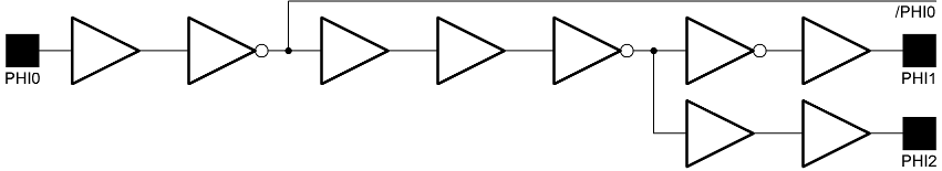
PHI2 is in phase with PHI0, while PHI1 is out of phase with it. Data from data bus are scanned when PHI2 goes down.
All internal timing signals are derived from /PHI0.
RDY pad and P1 and P2 signals
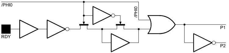
RDY is scanned when PHI1 is high. If RDY is low P1 stays high and P2 low till RDY goes high again.
P1 is in phase with PHI1, P2 is in phase with PHI2.
P1a, P2a, P1b, P2b and P1c signals
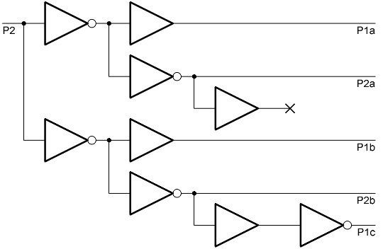
Various copies of P1 and P2 timing signals. P1 and P2 is almost not used in the chip logic, instead of them derived signals are used.
P1a and P2a are delayed compared to P1 and P2. P1b and P2b are very slightly delayed compared to P1a and P2a. P1c is slightly delayed compared to P1b.
Note as well that there is one unused output which probably is some residue from earlier stage of development.
T2, T3, T4, T5, T6, T7 and T6P1P2 timing signals
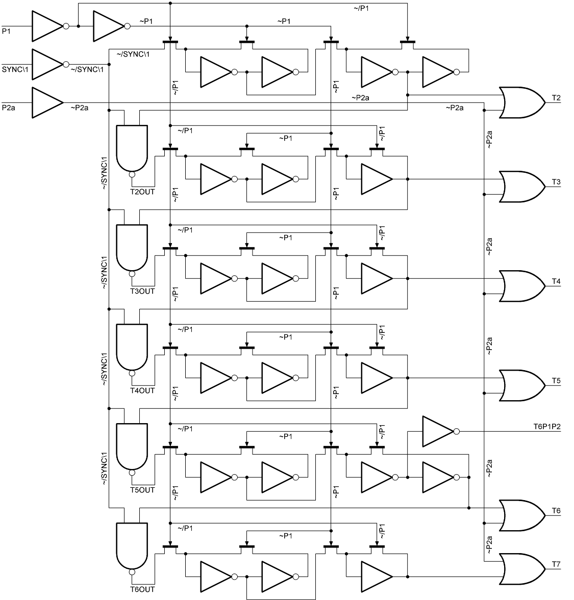
Maximum duration of 65CE02 instruction is 7 cycles. Minimum is 1 cycle. There is fetch-execute overlap of one cycle.
T2...T7 signals show in which cycle current instruction currently is. These signals together with content of the instruction register serve as inputs to the microcode ROM.
All the T* signals are high during P2 when the ROM is precharged. During P1 at most one of the T* signal is high. There is no T1 signal because in the first cycle fetch of the instruction occurs.
Real execution of the instruction starts in T2. The counter is reset by SYNC\1 signal which means that a new instruction has started.
If current instruction has 7 cycles the counter overflows and all T* signals are low during P1. But as all signals from ROM are delayed, including SYNC\1 the counter is properly reset anyhow.
T6P1P2 signal is high in sixth cycle only. It doesn't go up during P2 of other cycles like T6 signal does. It is used in interrupt and reset logic.
Example of described signals can be seen in the following table. Example shows executions of few instructions, note the fetch-execute overlap. As well note that I use the convention that full cycle starts with P1 and ends with P2.
| P1 | P2 | T2 | T3 | T4 | T5 | T6 | T7 | T6P1P2 | SYNC\1 | note |
| | X | X | X | X | X | X | X | | | finishing CLE |
| X | | | X | | | | | | | |
| | X | X | X | X | X | X | X | | X | fetching LDX #d8 |
| X | | X | | | | | | | X | |
| | X | X | X | X | X | X | X | | | reading data |
| X | | | X | | | | | | | |
| | X | X | X | X | X | X | X | | X | fetching ASW a16 |
| X | | X | | | | | | | X | |
| | X | X | X | X | X | X | X | | | reading low address |
| X | | | X | | | | | | | |
| | X | X | X | X | X | X | X | | | reading high address |
| X | | | | X | | | | | | |
| | X | X | X | X | X | X | X | | | reading low data |
| X | | | | | X | | | | | |
| | X | X | X | X | X | X | X | | | writing low data |
| X | | | | | | X | | X | | |
| | X | X | X | X | X | X | X | X | | reading high data |
| X | | | | | | | X | | | |
| | X | X | X | X | X | X | X | | | writing high data |
| X | | | | | | | | | | |
| | X | X | X | X | X | X | X | | X | fetching TXS |
| X | | X | | | | | | | X | |
| | X | X | X | X | X | X | X | | X | fetching TYS |
| X | | X | | | | | | | X | |
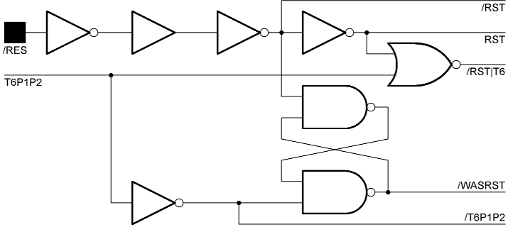
/RES pad, RST and /WASRST signals
Reset is an interrupt with highest priority.
RST and /RST signals are derived directly from /RES. When /RST is low SYNC\1 is forced high which effectively resets and stops timing counter and immediately interrupts current instruction. RST or /RST signal clears flag E, sets overflow flip flop, register B, register Z and puts value $01 into SPH register and immediately stops current write cycle.
/WASRST signal is used in several other parts of CPU. It is held low for 5 cycles following the end of external reset. It ensures that BRK instruction is fetched to the instruction register, it prevents CPU from writing return address to the stack during the executing this BRK instruction and it creates correct jump vector.
/RST|T6 is used for clearing NMI flip flop in a similar way as T6P1P2 is used for clearing RST flip flop.
/NMI pad, /WASNMI signal
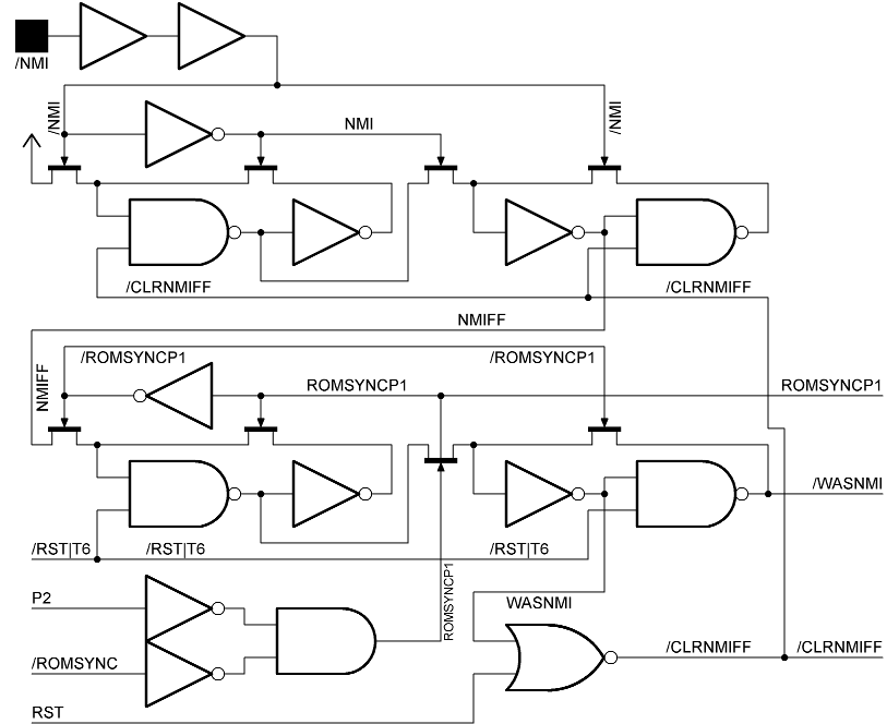
NMI is an interrupt with priority lower than RES. Everytime NMI and RES occur simultaneously RES overrides NMI and takes over.
NMIFF signal is output from NMI latch which is set at high to low transition on the NMI pad. This latch remembers the NMI condition until it is served or cleared by reset.
NMIFF propagates to second latch at ROMSYNCP1 which is high during P1 of the fetching cycle which should ensure that NMI starts after finishing current instruction. Unfortunately this seems like a design flaw, because several instructions like NOP, ASL A, TSY, etc. which last one cycle are not finished by ROMSYNC signal but by PRESYNC signal which will be explained later.
Consequence of this is that if there are several instructions with duration one cycle in a row (like few consecutive NOPs) NMI starts after first instruction longer than one cycle.
Second latch holds /WASNMI signal which like /WASRST signal lasts 5 cycles and creates correct vector and ensures that BRK instruction is fetched instead of the next instruction. This latch is cleared (forced high) by /RST|T6 which means that /WASNMI condition could be canceled by reset as well.
And at the end - RST or WASNMI condition will reset the latch holding NMIFF signal by using /CLRNMIFF signal.
There is one more issue with NMI. As the NMIFF signal is propagated at positive edge of ROMSYNCP1 the /WASNMI signal goes low at P1 of fetch cycle. Unfortunately this prevents PC to increment before fetching next instruction which is BRK. So wrong return address is pushed on the stack. The address is lower by one than it should be. This error is worth to be confirmed in the real hardware.
All mentioned signals are shown in the table below.
| P1 | P2 | ROMSYNCP1 | NMIFF | T6P1P2 | /WASNMI | PC | note |
| X | | | X | | X | 001F | |
| | X | | X | | X | 0020 | fetching NOP |
| X | | | X | | X | 0020 | |
| | X | | X | | X | 0021 | fetching LDA #d8 |
| X | | | X | | X | 0021 | |
| | X | | X | | X | 0022 | reading argument |
| X | | X | | | | 0022 | PC not incremented |
| | X | | | | | 0022 | fetching BRK |
| X | | | | | | 0022 | |
| | X | | | | | 0022 | |
| X | | | | | | 0022 | |
| | X | | | | | 0022 | writing PCH |
| X | | | | | | 0022 | |
| | X | | | | | 0022 | writing PCL |
| X | | | | | | 0022 | |
| | X | | | | | 0022 | writing flags |
| X | | | | X | X | 0022 | |
| | X | | | X | X | 0022 | |
| X | | | | | X | 0022 | |
| | X | | | | X | 00FE | |
| X | | X | | | X | 00FE | |
| | X | | | | X | 00FE | fetching RTI |
/IRQ pad, /WASIRQ signal
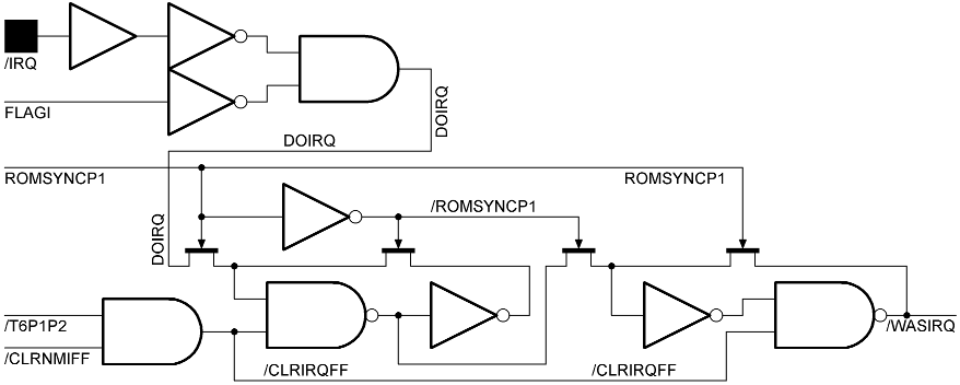
FLAGI is output from flag I flip flop. Interrupt is recognized only when flag I is zero. Unlike NMI the IRQ is not remembered by flip flow so it could be missed.
There is the same problem with ROMSYNC signal as with NMI signal. Long sequence of one clock instructions will postpone the IRQ. Unlike NMIFF signal the DOIRQ is propagated at negative edge of ROMSYNCP1. So /WASIRQ starts at P2 of fetch cycle, PC is incremented and the return address on the stack is correct.
If NMI and IRQ occur at the same time, NMI has higher priority, so /CLRNMIFF signal prevents /WASIRQ signal to occur.
Again all mentioned signals are shown in the table below.
| P1 | P2 | ROMSYNCP1 | T6P1P2 | /WASIRQ | PC | note |
| X | | | | X | 001F | |
| | X | | | X | 0020 | fetching NOP |
| X | | | | X | 0020 | |
| | X | | | X | 0021 | fetching LDA #d8 |
| X | | | | X | 0021 | |
| | X | | | X | 0022 | reading argument |
| X | | X | | X | 0023 | PC incremented |
| | X | | | | 0023 | fetching BRK |
| X | | | | | 0023 | |
| | X | | | | 0023 | |
| X | | | | | 0023 | |
| | X | | | | 0023 | writing PCH |
| X | | | | | 0023 | |
| | X | | | | 0023 | writing PCL |
| X | | | | | 0023 | |
| | X | | | | 0023 | writing flags |
| X | | | X | X | 0023 | |
| | X | | X | X | 0023 | |
| X | | | | X | 0023 | |
| | X | | | X | 00FE | |
| X | | X | | X | 00FE | |
| | X | | | X | 00FE | fetching RTI |
/SO pad, SETFLAGV signal
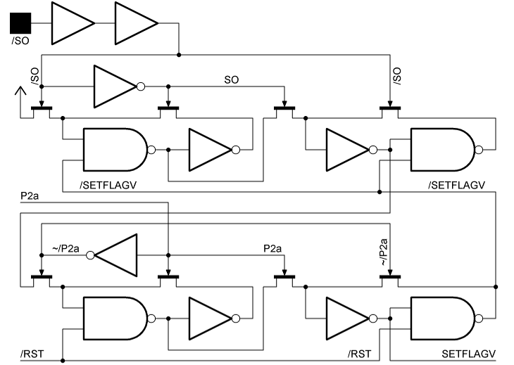
As the /SO input goes low, logical one is propagated from the first flip flop to the second one. At the next P2 the SETFLAGV is set high for the P2 and P1 of the next cycle. /SETFLAGV is used for clearing the first flip flop.
All mentioned signals are shown in the table below.
| P1 | P2 | /SO | SETFLAGV |
| X | | X | |
| | X | X | |
| X | | | |
| | X | | X |
| X | | | X |
| | X | | |
| X | | X | |
| | X | X | |
SYNC pad, SYNC and SYNC\1 signals
ROM signals: /ROMSYNC
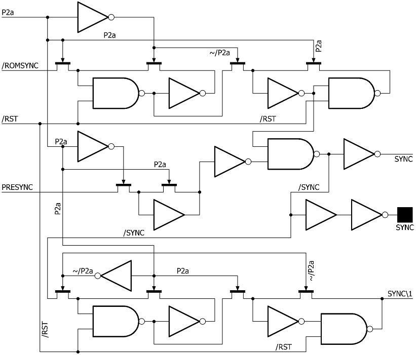
This part of the CPU combines /ROMSYNC and PRESYNC signals. /ROMSYNC designates the real last cycle of the instruction which is executed at the same time as the fetch of the next instruction. This signal goes from internal ROM. PRESYNC is output from special circuit which identifies instructions with duration of one cycle. All will be explained later.
During the reset SYNC is high. SYNC\1 is SYNC delayed by half cycle. SYNC is high during P1 and P2 of the fetch cycle, while SYNC\1 is high during P2 of the fetch cycle and P1 of the next cycle. SYNC\1 logically belongs to the timing logic described above, by which it is exclusively used but physically is created near SYNC pad, that's why it is here.
All mentioned signals are shown in the table below.
| P1 | P2 | PRESYNC | /ROMSYNC | SYNC | SYNC\1 | note |
| X | | | X | | | |
| | X | | | | | |
| X | | | | X | | |
| | X | | X | X | X | fetching CLI |
| X | | | X | | X | |
| | X | | | | | |
| X | | | | X | | |
| | X | X | X | X | X | fetching NOP |
| X | | X | X | X | X | |
| | X | | X | X | X | fetching LDA #d8 |
| X | | | X | | X | |
R/W pad, W/R signal
ROM signals: ROMWR
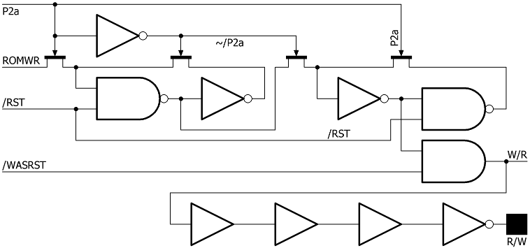
ROMWR signal is generated by the ROM at P1P2. It is propagated to output R/W pad and to W/R signal one cycle later. The writing cycle is immediately suppressed by reset. As well when reset sequence is running (by using BRK instruction) pushing the return address on the stack is suppressed as well by /WASRST signal.
ROMWR signal is high during the reset but R/W is forced low by /RST signal.
| P1 | P2 | ROMWR | W/R | R/W |
| X | | | | X |
| | X | | | X |
| X | | X | | X |
| | X | X | | X |
| X | | | X | |
| | X | | X | |
| X | | | | X |
| | X | | | X |
D* pads (data bus), D* signals
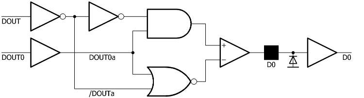
Data bus is bidirectional, no other pad is bidirectional. It consists of input part which is shown in the right side of the schematic. There is only protecting diode and buffer there. The D0 to D7 signals go to instruction register and DIN (data in) register.
The output part (shown left) is slightly more complicated as the output has to have tri-state logic. There is DOUT signal which enables output when it is high. When it is low the output is disabled. DOUT0 is a signal meaning bit to be output, for DOUT0 is is bit 0. It goes from DOUT (data out) register.
Obviously there are 8 copies of this schematic, one for each D* pad.
Register DIN
Derived ROM signals: RDDIN, WRDIN
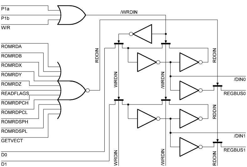
Register DIN (data in) holds last data read from external data bus. External data bus is read everytime when it is not used for writing data. The data are read during P2 and are held (and valid) during P1. Note the use of both clock signals P1a and P1b. Probable reason is to make time slot for reading data during P2 little bit shorter.
Data stored in register DIN may be put on the register bus REGBUS (REGBUS0 - REGBUS7 signals) by the use of signal RDDIN. RDDIN is made by NORing another 11 signals (see above). Basically - if nothing else is being put on the register bus (registers A, B, X, Y, Z, flags, PCH, PCL, SPH, SPL or vector) the content of the DIN register is put there.
There are as well negated outputs from DIN register (signals /DIN0 - /DIN7) which go directly to ALU.
See also transistor schematic of DIN register here. It's visible that 11-input NOR gate is in fact implemented as 6-input NOR and 5-input NOR which are NANDed together there. The signal goes thru buffer and it's used in all 8 bits of the register.
Of course the register is not fully shown in the schematic, only 2 bits (or 1 bit in transistor version) is shown. Rest of the bits is analogous.
Register DOUT and DOUT signal
ROM signals: ROMWRDOUT
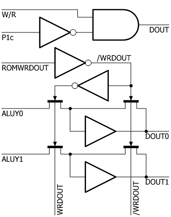
Register DOUT (data out) holds data to be written out to the external data bus. ALU is the only source of data to be written. ROMWRDOUT takes place during P2 and P1 just before writing valid data in P2 of write cycle when DOUT signal forces data bus to be in output mode.
| P1 | P2 | ROMWR | W/R | R/W | ROMWRDOUT | DOUT |
| X | | | | X | | |
| | X | | | X | | |
| X | | X | | X | | |
| | X | X | | X | X | |
| X | | | X | | X | |
| | X | | X | | | X |
| X | | | | X | | |
| | X | | | X | | |
Instruction register part 1 and IR* signals
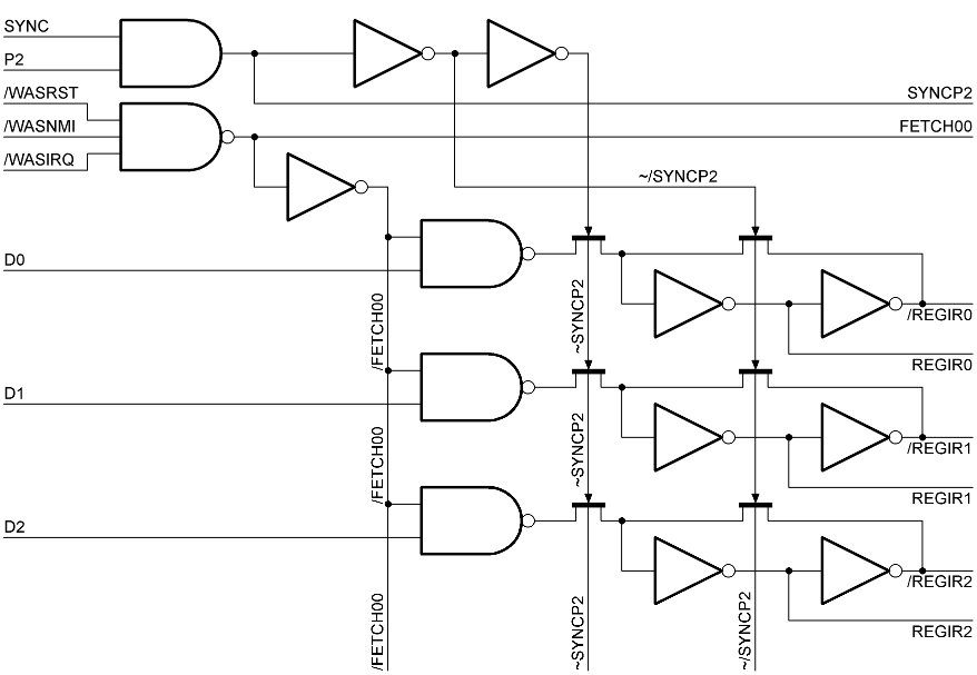
The instruction register is loaded during P2 of the SYNC cycle. /WASRST, /WASNMI and /WASIRQ cause that BRK is fetched instead of the current instruction. FETCH00 signal also prevents PC from incrementing. Note the error in NMI processing.
Instruction register part 2 and INSB4, INSB5, INSB6 signals
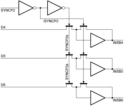
Alternative part of the instruction register. It stores bit 4, 5 and 6. It is used for bit decoding for BBR and BBS instructions (opcodes 0F, 1F, 2F ... EF, FF) which is done in ALU. I am not sure why REGIR4, REGIR5 and REGIR6 signals are not used instead.
PRESYNC signal
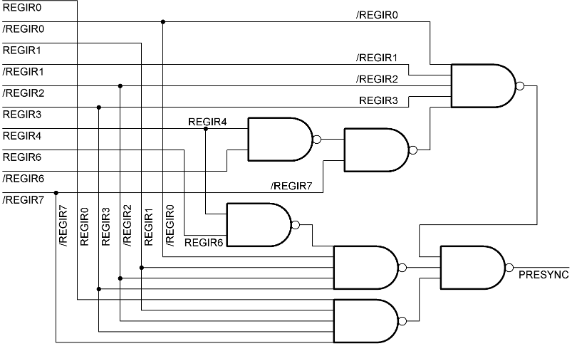
PRESYNC logic is described in US patent no 5,088,035 - System for accelarating execution of program instructions by a microprocessor from Feb. 11, 1992. Note that input signals contained in the schematic in this patent (bits of instruction) are inverted.
PRESYNC is high for the following opcodes: 0A, 0B, 18, 1A, 1B, 2A, 2B, 38, 3A, 3B, 4A, 4B, 5B, 6A, 6B, 7B, 88, 8A, 98, 9A, A8, AA, B8, BA, C8, CA, D8, E8, EA, F8. All these instructions last one cycle.
Internal ROM precharge logic
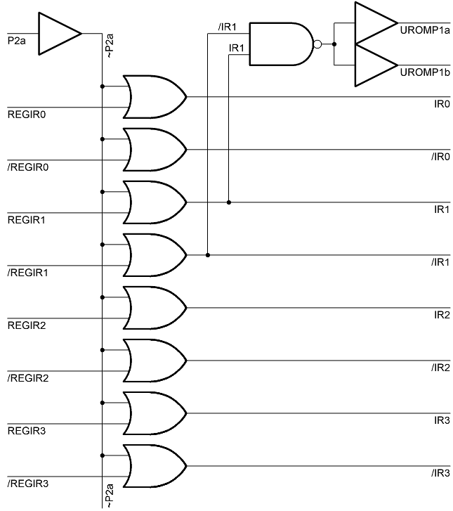
Outputs from instruction register are ORed with P2 signal and amplified because during P2 the ROM is precharged. Additional clock signals UROMP1a and UROMP1b are derived from IR1 and /IR1. They are in sync with P1. During P2 signal UROMP1b opens the PMOS transistors which connect the AND part of the ROM with power. UROMP1a opens the NMOS transistors and connects the AND part with ground during P1.
Internal ROM (PLA)
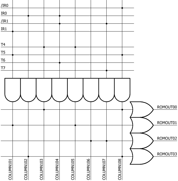
See explanation and listing of the internal ROM content here. Read it before you continue.
Schematic above is highly simplified. Only part of the signals described in previous link is shown. Note that connections in the AND and OR matrix shown in the above schematic are rather educational than real so do not agree with the ROM listing in last link.
See also transistor schematic of AND part of PLA here to see how precharge logic works. There are two pull-ups for every column (AND line). One strong which is open every P2 phase and one weak which is handled by inverted output from each NAND line.
See also transistor schematic of OR part of PLA here to see the other part of PLA. There is analogous trick with two pull-ups.
If there is to be too many transistors (over 52) in OR line, this line is separated into two OR lines which are ORed together. Well, in reality into two NOR lines which are NANDed. See here how it is implemented.
ROM outputs
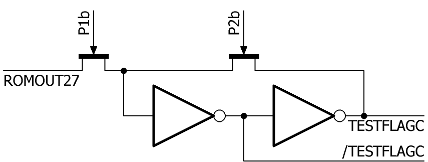
As explained in above mentioned document the ROMOUT signals are prolonged and delayed. Basically there are three types of such actions. The first one (schema above) just prolongs the signal from P1 to both P1 and P2 phases (whole T cycle).
Example of this is in the table below. Note that sometimes the output signal has positive logic, sometimes it is inverted and sometimes both signals are used.
| P1 | P2 | ROMOUT27 | TESTFLAGC |
| | X | | |
| X | | X | X |
| | X | | X |
| X | | | |
| | X | | |
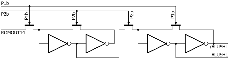
The second type of delay circuit delays the ROM signal by one phase. Again both inverted and non-inverted signals may be produced.
| P1 | P2 | ROMOUT14 | ALUSHL |
| | X | | |
| X | | X | |
| | X | | X |
| X | | | X |
| | X | | |
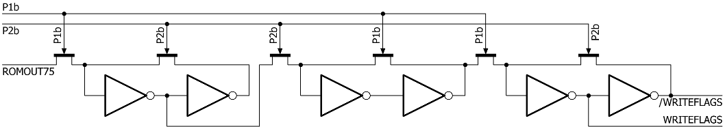
The third type of delay circuit delays the ROM signal by two phases. Everything else is analogous.
| P1 | P2 | ROMOUT75 | WRITEFLAGS |
| | X | | |
| X | | X | |
| | X | | |
| X | | | X |
| | X | | X |
Register A
ROM signals: ROMRDA, ROMWRA
Register A is connected to ALU output at its input side and to register bus at its output side. The content of the register can be read by ROMRDA singal, data can be written to A register by ROMWRA signal. Note that writing takes place at P1 phase, i.e. writing signal is shortened from P2P1 duration to its second half only.
Register A is implemented as master slave latch. New value appears at its input at the high-low transition of WRA signal. This allows implementing instructions like INC A without any temporary register at ALU input.
Transistor version of the schematic is here.
Register X
ROM signals: ROMRDX, ROMWRX

Register X is analogous to register A.
Register Y
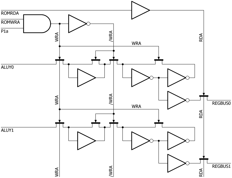
ROM signals: ROMRDY, ROMWRY
Register Y is analogous to register A.
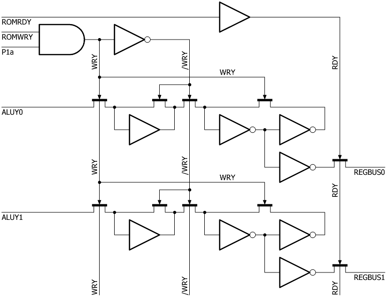
Register Z
ROM signals: ROMRDZ, ROMWRZ
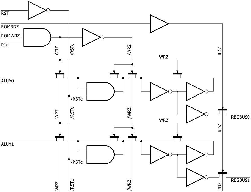
Register Z is analogous to register A. With one important difference - during the reset the register is cleared. Transistor version of the schematic is here.
Register B
ROM signals: ROMRDB, ROMWRB
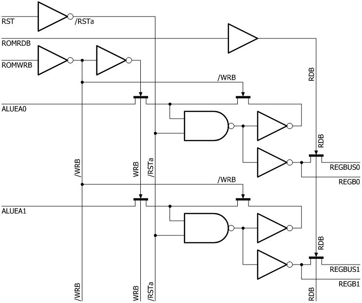
Register B is a transparent latch, not a master slave flip-flop, because it is not involved in aritmetic operations. It also has (besides the output to register bus) one direct connection to ABH register thru REGB bus. This register is cleared during reset as well.
The inputs are not taken from common ALU output (ALUY* bus) but from ALUEA* bus, which is used for effective address calculation. It will be shown later.
ALU input A
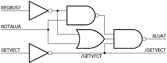
ROM signals: NOTALUA, GETVECT
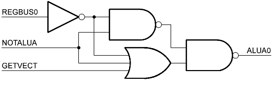
First argument of the ALU. It can be 1) content of the register bus (REGBUS), 2) low 8 bits of the vector ($FA for NMI, $FC for reset and $FE for IRQ/BRK) this feature is used by BRK instruction and it is activated by GETVECT signal, and finally 3) negated register bus, which is used by TRB instruction and activated by NOTALUA signal.
NOTALUA and GETVEC are never high at the same time.
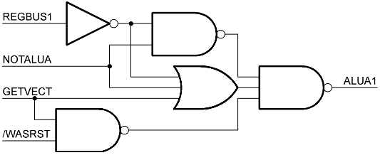
Here the low /WASRST signal drives the ALUA1 low if GETVECT signal is high.

Here the low /WASNMI signal drives the ALUA2 low if GETVECT signal is high.
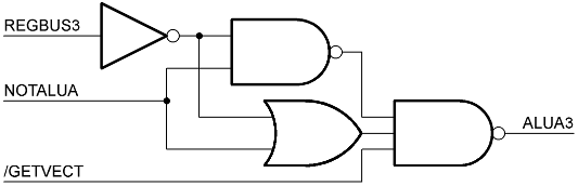
Schematic above is analogous for bits 3, 4, 5 and 6.
This bit differs only in one detail - /GETVECT signal is created there.
Possible ALU A inputs are recapitulated below:
| GETVECT | NOTALUA | ALU A input |
| | | register bus |
| | X | inverted register bus |
| X | | lower byte of a vector |
| X | X | N/A |
ALU input B
ROM signals: GETALUB, GENBIT, NOTALUB
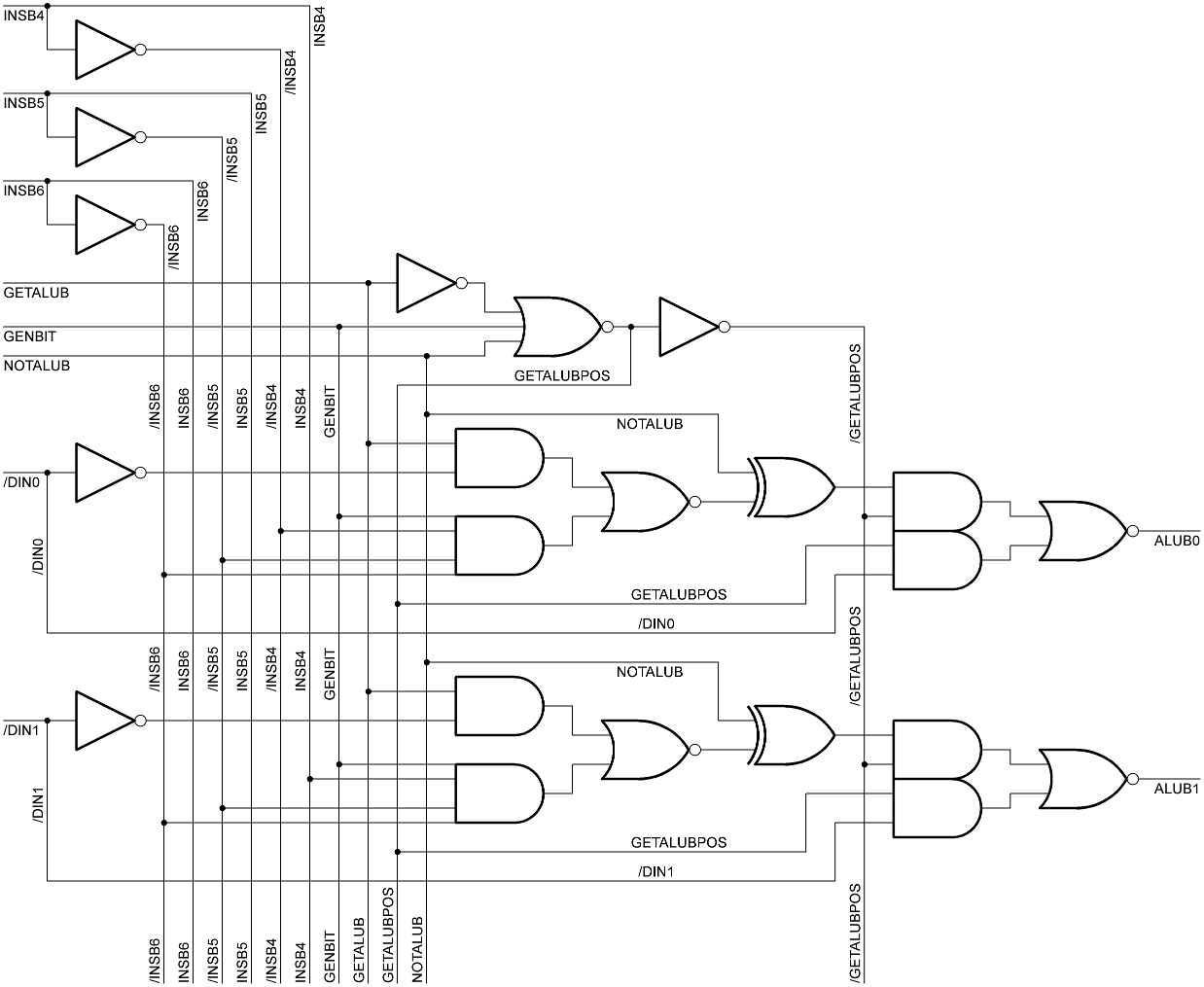
There are three different sources of data which can be put to ALU B input and both of them can be negated. First of them is $00 if none of three control signals (GETALUB, GENBIT and NOTALUB) is high. It can be negated by NOTALUB signal to $FF.
Second very obvious source of the data is DIN (data in) register activated by GETALUB signal. As well its content can be negated by NOTALUB signal. Negation of DIN register is mostly used for subtraction.
Third source is activated by GENBIT signal. It is used by RMB*, SMB*, BBR* and BBS* instructions. It sets just one bit based on bits 4, 5 and 6 of instruction register. This source can also be negated by NOTALUB. This negation is used by RMB* instructions.
Note that the most common combination where GETALUB is 1, NOTALUB is 0 and GENBIT = 0 has its own path AND-NOR by use of GETALUBPOS signal. Probably because of the increased speed of such solution.
Possible ALU B inputs are recapitulated below:
| GENBIT | GETALUB | NOTALUB | ALU B input |
| | | | zeroes ($00) |
| | | X | ones ($FF) |
| | X | | DIN register |
| | X | X | inverted DIN register |
| X | | | bit set |
| X | | X | bit cleared |
| X | X | | N/A |
| X | X | X | N/A |
ALU carry (ALUC) and carry in (CARRYIN)
ROM signals: CINDLDC, CINFLAGC, CINONE
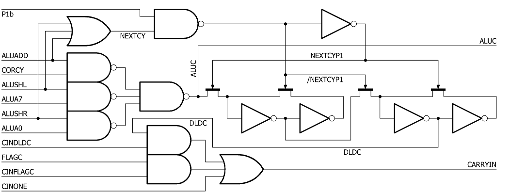
There are two parts of the circuit above. First one creates possible content of the carry flag (ALUC signal) if current instruction modifies it via MODFLAGC signal which will be explained below.
There are three possible sources of carry flag:
- CORCY signal (decimal adjusted/corrected carry) which contains carry bit from adder decimal adjusted if applicable. In further explanation it becomes understandable that while computing (adding) effective address there is no decimal adjustment but carry is still incorporated in CORCY signal. Note that ALUADD signal is used not only for ADC and similar instructions but for effective address calculations as well.
- Bit 7 of the ALU A input for left shift/rotations (controlled by ALUSHL signal).
- Bit 0 of the ALU A input for right shift/rotations (controlled by ALUSHR signal).
Besides in the carry bit itself, the possible carry is always saved in master slave flip flop for potential use in 16-bit operations by using DLDC (delayed carry) signal.
The other part of the circuit above creates CARRYIN signal for ALU. Carry in coud be:
- Flag C (controlled by CINFLAGC signal)
- 1 (controlled by CINONE signal)
- Delayed carry for higher byte of 16-bit operations (controlled by CINDLDC signal)
ALU part 1 - basic operations
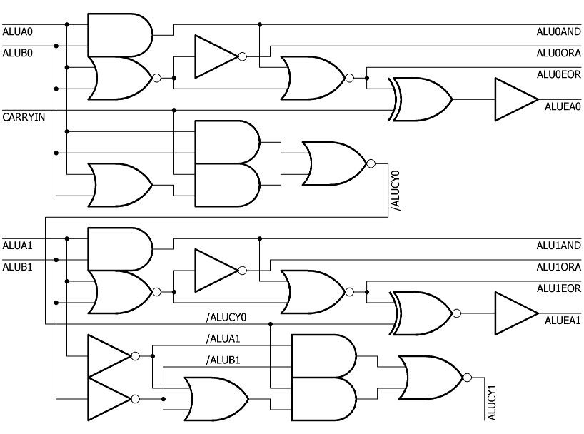
Basic part of the ALU. Performs AND, OR, XOR operations and adding. Decimal correction is explained later. Outputs ALUEA* are used also for effective address calculation so they go as well directly to PC, AB, AD and B registers. In this case the result is never decimal adjusted even if D flag is set.
ALU part 2 - decimal correction control
ROM signals: ALUADCINS
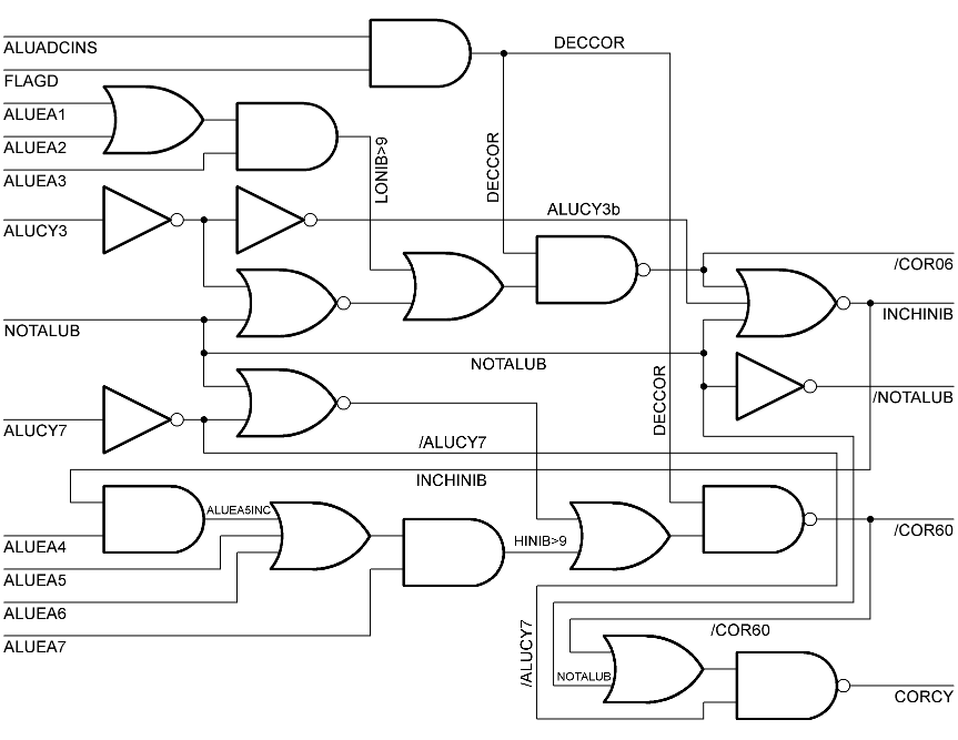
This circuit checks if decimal correction should be done or not. The whole logic is enabled by DECCOR signal which is high when flag D is set and when ALU is computing ADC or SBC which can be corrected.
Signal /COR06 says if $06 should be added to / subtracted from the result (correct low nibble) and signal /COR60 says that $60 should be added to / subtracted from the result (correct high nibble).
INCHINIB signal causes the high nibble to increment. It is necessary when there was no carry from low nibble to high nibble and low nibble was corrected by adding $06.
CORCY signal is corrected carry bit. When high nibble was corrected ($60 added) the carry should be set. This signal is used in ALU carry in circuit.
Table below shows combinations of input and output signals for low nibble. LONIB>9 means that lower nibble is higher than 9 (i.e. $A-$F), analogously HINIB>9 means that high nibble contains number higher than 9. Of course DECCOR must be high. Meaning of green and red cells is explained below.
| NOTALUB | ALUCY3 | LONIB>9 | /COR06 | INCHINIB |
| | | | X | |
| | | X | | X |
| | X | | | |
| | X | X | | |
| X | | | X | |
| X | | X | | |
| X | X | | X | |
| X | X | X | | |
An explanation of decimal correction of addition is shown in the table below, NOTALUB signal is low (we are adding). For all 10*10 combinations of possible addends (say low nibble is shown) there is sum colored in three different colors.
White - sum is correct and does not need to be further corrected. LONIB>9 and ALUCY3 are low. So /COR06 is high (inactive).
Yellow - sum contains number outside the decimal range ($A-$F). LONIB>9 is high and ALUCY3 is still low. $6 has to be added to the low nibble. As well high nibble has to be incremented which is done by INCHINIB signal. Thus $5 + $5 = $A. Nocarry, higher than $9, thus $6 is added, the result is $10, so high nibble has to be incremented. /COR06 is low (active).
Orange - carry from low nibble to high nibble occurred thus high nibble was already incremented so doesn't need to be incremented again. LONIB>9 is low and ALUCY3 is high. Low nibble has to be corrected so /COR06 is low (active). For example $8 + $8 = $10, after correction (adding $6) the result is $16.
Also note that combination LONIB>9 is high and ALUCY3 is high never occurs. Thus does not matter what /COR06 and INCHINIB signals are, in the table above their values in such case are marked green.
| | 0 | 1 | 2 | 3 | 4 | 5 | 6 | 7 | 8 | 9 |
| 0 | 00 | 01 | 02 | 03 | 04 | 05 | 06 | 07 | 08 | 09 |
| 1 | 01 | 02 | 03 | 04 | 05 | 06 | 07 | 08 | 09 | 0A |
| 2 | 02 | 03 | 04 | 05 | 06 | 07 | 08 | 09 | 0A | 0B |
| 3 | 03 | 04 | 05 | 06 | 07 | 08 | 09 | 0A | 0B | 0C |
| 4 | 04 | 05 | 06 | 07 | 08 | 09 | 0A | 0B | 0C | 0D |
| 5 | 05 | 06 | 07 | 08 | 09 | 0A | 0B | 0C | 0D | 0E |
| 6 | 06 | 07 | 08 | 09 | 0A | 0B | 0C | 0D | 0E | 0F |
| 7 | 07 | 08 | 09 | 0A | 0B | 0C | 0D | 0E | 0F | 10 |
| 8 | 08 | 09 | 0A | 0B | 0C | 0D | 0E | 0F | 10 | 11 |
| 9 | 09 | 0A | 0B | 0C | 0D | 0E | 0F | 10 | 11 | 12 |
An explanation of decimal correction of subtraction is shown in the table below, NOTALUB signal is high (we are subtracting). Minuends are in rows, subtrahends are in columns. There is no need for DECHINIB signal as the higher nibble is always correctly decreased.
The logic of subtraction is the same as in 6502. Second ALU argument is negated by using NOTALUB and carry flag is not negated internally, thus borrow logic is different than in Z80 let's say.
The cells in table below contain three colors like table above.
White - result is correct and does not need to be further corrected. ALUCY3 set (i.e. no borrow) and LONIB>9 is low. /COR06 is correctly high (inactive).
Yellow - result contains number outside the decimal range ($A-$F). LONIB>9 is high and ALUCY3 is low (borrow). $6 has to be subtracted from the low nibble. High nibble is already correctly decremented. Thus $11 - $4 = $D. After $6 is subtracted, the correct result is $7 is obtained. /COR06 is low (active).
Orange - high niblle is already correctly decremented, ALUCY3 is low (borrow) and LONIB>9 is low as well. Lower nibble should be corrected but in fact it ISN'T. The /COR06 signal is high and thus inactive. This is 65CE02 error which produces wrong results for subtraction in decimal mode. For example $11 - $8 = $9. This value should be further corrected by subtracting $6 to correct value $3 but in fact it isn't. This fact is shown in above table of /COR06 signal by the red cell. This error was confirmed for both 65CE02 and 4510 CPUs by (.... list of names ...).
Also note that combination LONIB>9 is high and ALUCY3 is high never occurs. Thus does not matter what /COR06 and INCHINIB values are in such case, in the table above their values are marked green.
| | 0 | 1 | 2 | 3 | 4 | 5 | 6 | 7 | 8 | 9 |
| 10 | 10 | 0F | 0E | 0D | 0C | 0B | 0A | 09 | 08 | 07 |
| 11 | 11 | 10 | 0F | 0E | 0D | 0C | 0B | 0A | 09 | 08 |
| 12 | 12 | 11 | 10 | 0F | 0E | 0D | 0C | 0B | 0A | 09 |
| 13 | 13 | 12 | 11 | 10 | 0F | 0E | 0D | 0C | 0B | 0A |
| 14 | 14 | 13 | 12 | 11 | 10 | 0F | 0E | 0D | 0C | 0B |
| 15 | 15 | 14 | 13 | 12 | 11 | 10 | 0F | 0E | 0D | 0C |
| 16 | 16 | 15 | 14 | 13 | 12 | 11 | 10 | 0F | 0E | 0D |
| 17 | 17 | 16 | 15 | 14 | 13 | 12 | 11 | 10 | 0F | 0E |
| 18 | 18 | 17 | 16 | 15 | 14 | 13 | 12 | 11 | 10 | 0F |
| 19 | 19 | 18 | 17 | 16 | 15 | 14 | 13 | 12 | 11 | 10 |
Table below shows combinations of input and output signals for high nibble. HINIB>9 means that lower nibble is higher than 9 (i.e. $A-$F) and of course DECCOR must be high. CORCY is decimally corrected carry which is copy of the ALUCY7 whith the exception of addition when high nibble contains values $A - $F which has to be corrected. In that case CORCY has to be high.
The table is analogous to the table above describing signals for low nibble. So it contains the same don't care combinations marked green and the same design error causing wrong results for decimal subtraction.
| NOTALUB | ALUCY7 | HINIB>9 | /COR60 | CORCY |
| | | | X | |
| | | X | | X |
| | X | | | X |
| | X | X | | X |
| X | | | X | |
| X | | X | | |
| X | X | | X | X |
| X | X | X | | X |
ALU part 3 - decimal correction low nibble
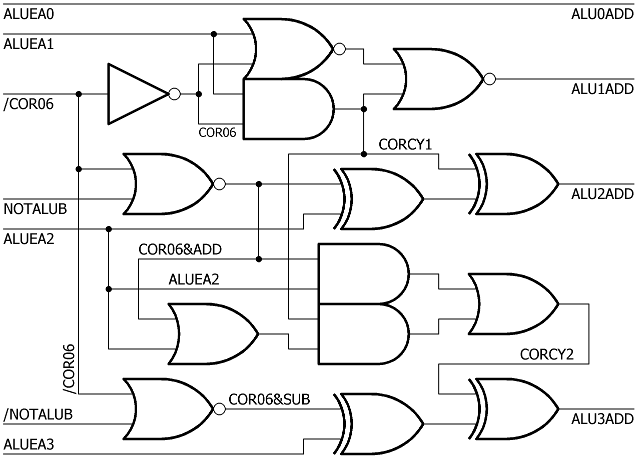
This circuit corrects the lower nibble. If /COR06 is high nothing happens. If it is low (active) and NOTALUB is low $6 is added to the result of adding. If NOTALUB is high $A is added - i.e. $6 is subtracted.
No carry to the higher nibble is needed as it is solved by INCHINIB signal described above.
ALU part 4 - decimal correction high nibble
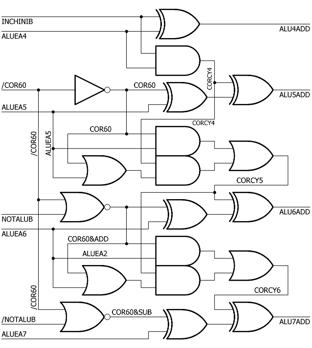
This circuit corrects the higher nibble. It is analogous to the correction of the lower nibble. It can as well increment the higher nibble if INCHINIB signal is high.
ALU part 5 - multiplexer
ROM signals: ALUADD, ALUSHL, ALUSHR, ALUAND, ALUEOR
Derived ROM signals: ALUORA
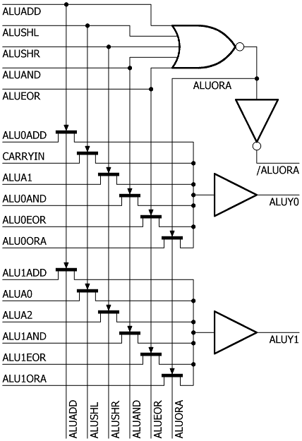
This choose one of the ALU outputs depending on the current instruction. Note that ALUORA signal is not generated in ROM, it is just the idle option, it is high when nothing other (ALUADD, ALUSHL, ALUSHR, ALUAND, ALUEOR) is requested. Also note that besides ALUY* outputs ALU still has ALUEA* outputs for effective address calculation.
This circuit as well contains logic for rotations and shifts both left and right.
Sixth and seventh bit of the multiplexer. Provision for shifts and rotations is shown for the top two bits of the data bus.
ALU zero (ALUZ)
ROM signals: /ROMWORDZ
Similarly to carry flag, the zero flag circuit has also provision for 16-bit operations. The Z flag is put into flip flop during of P1 of non-ORA ALU operation. ORA operation is either true ORA operation or just idle ALU cycle. But it does not matter because there is no 16-bit ORA instruction. Later during next ALU non-ORA operation saved Z flag may be ANDed with the zero flag of higher byte of 16-bit word. This functionality is controlled by /ROMWORDZ signal and it is used during ASW, ROW, DEW and INW instructions.
ALU overflow (ALUV) and negative (ALUN)
INSBIT signal identifies BIT instruction (ALU performs AND operation and flag V is to be modified), because behavior of N and V flags is different in BIT instruction.
Flag N is copy of bit 7 of the ALU result or bit 7 of ALU B input in the case of BIT instruction when DIN register is put there. Note that three NANDs at the top of the schematic work as AND-OR.
Flag V is calculated as (ALUA7 XOR ALUY7) AND (ALUB7 XOR ALUY7) i.e. is high when sign of the both ALU inputs are the same (ALUA7 = ALUB7) and the sign of the result is different (ALUY7 <> ALUA7). Note that this logic works for subtraction as well as in this case ALU B input is not subtrahend but its negation. And in the case of BIT instruction the V flag is just copy of bit 6 of ALU B input. This is shown in the table below:
| ALUA7 | ALUB7 | ALUY7 | ALUV |
| | | | |
| | | X | X |
| | X | | |
| | X | X | |
| X | | | |
| X | | X | |
| X | X | | X |
| X | X | X | |
FLAG B (FLAGB)
ROM signals: READFLAGS
Flag B does not have any flip flop as it is generated only when pushed on the stack. It is low only when FETCH00 is high, i.e. during NMI and IRQ. During RES it is low as well but the writing of the P register is supressed. In other cases (BRK, PHP) the B flag is set.
READFLAGS signal is used by BRK and PHP instructions.
FLAG E (FLAGE)
ROM signals: SETFLAGE, CLRFLAGE

Flag E has its own flip flop. It can be set and reset and is set during reset. As well it cannot be modified (unlike the flags described below) which means that it cannot be changed by PSP or RTI instructions.
FLAG D (FLAGD)
ROM signals: SETFLAGD, CLRFLAGD, WRITEFLAGS

Flag D has its own flip flop. It can be set and reset. Unlike flags B and E and like all the other flags it can be modified which means it is changed by PSP and RTI instructions.
FLAG I (FLAGI)
ROM signals: SETFLAGI, CLRFLAGI
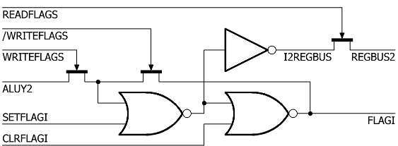
Flag I is analogous to flag D.
FLAG N (FLAGN)
ROM signals: MODFLAGN
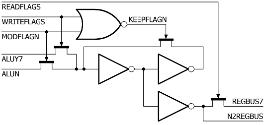
Flag N does not have SET and CLR functionality. On the other hand it can be modified directly from ALU by ALUN signal when MODFLAGN is high.
FLAG Z (FLAGZ)
ROM signals: MODFLAGZ
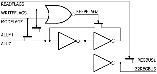
Flag Z is analogous to flag N.
FLAG V (FLAGV)
ROM signals: MODFLAGV, CLRFLAGV
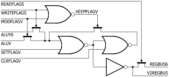
Flag V is similar to flag N. But it has SET and CLR functionality. CLRFLAGV is generated by ROM (CLV instruction) while SETFLAGV is generated by external input signal /SO. See above.
FLAG C (FLAGC)
ROM signals: MODFLAGC, SETFLAGC, CLRFLAGC
Flag C is similar to flag V. There is one important difference it is stored in master slave latch because it could be input to the ALU and stored from the ALU at the same time.
FLAG evaluation, CONDMET signal
ROM signals: TESTFLAGC, TESTFLAGN, TESTFLAGV, TESTFLAGZ, BBSRx, ONFLAG0
As the transistor implementation of this circuit is somewhat unusual see transistor schematic here as well. Note the implementation of XOR gate and also how the flag signals are put together.
If no flag is to be tested CONDMET signal is high. If a flag is tested its value is copied during P2 into a latch where it is during next P1 phase.
If ONFLAG0 is high the flag is tested for zero (BBS, BPL, BVC, BCC, BNE) and inverted value of the tested flag is put into the latch.
Low signal CONDMET prevents new value to be copied into PC register.
Register ADL
ROM signals: ROMWRADL, ROMADOUT
ADL register is lower part of AD register which is one of the four address registers. The other three are AB, PC and SP. Their content can be sent to address bus. In the case of AD register it is via ROMADOUT signal. ADL register has also direct connection to PCL register via ADL* signals as it serves as temporary register in 16-bit jumps and branches.
It is also used as an address register for effective address calculation in (a8,X); (a8),Y; (a8),Z and (r8,SP),Y addressing modes. The register can be written to from ALUEA* bus. It is only simple latch as it never serves as a source of data for ALU.
Register ADH
ROM signals: ROMWRADH
This is higher part of AD register. It is used in effective address calculation in (a8,X); (a8),Y; (a8),Z and (r8,SP),Y addressing modes. It can only be put to address bus and cannot be written anywhere else.
Register ABL
ROM signals: ROMWRAB, ROMABOUT, ROMINCAB
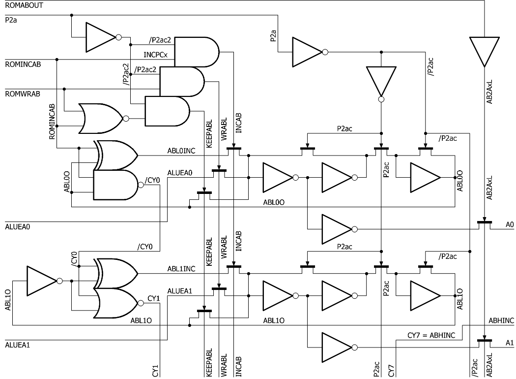
Register AB has its own incrementer. It can be written to from ALUEA* bus (when ROMWRAB is high) or incremented (when ROMINCAB is high). It is written to or incremented at the end of P1.
AB is used for zero (base) page addressing. ABL holds the lower byte of the address and ABH register holds copy of B register. Besides that AB is used for a16,X; a16,Y; (r8,SP),Y; (a16) and (a16,X) addressing modes.
Incrementing ability of AB is used when two successive memory locations should be read. I.e. by (a8,X); (a8),Y; (a8),Z; (r8,SP),Y; (a16); (a16,X) addressing modes and by INW, DEW, ASW, ROW and BRK instructions.
Signal ABHINC causes incrementing of ABH register if not suppressed by /INHABHINC signal. ABHINC is in fact CY7 signal which is the carry bit going out from the 7th bit of the incrementer.
Register ABL can be output to address bus (A*) using signal ROMABOUT. While feedback to incrementer comes from slave flip-flop, the output to the address bus comes from master stage so that it can be put there ahead - in the middle of PHI1 phase.
Register ABH
ROM signals: /INHABHINC, ROMWRABH
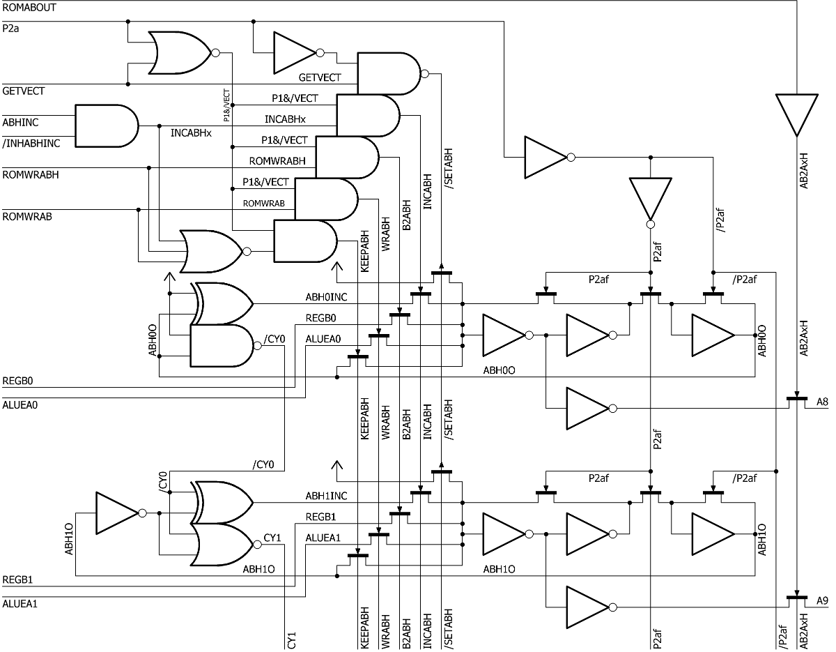
Register ABH is higher part of AB. It can be written to from B register via REGB* bus when ROMWRAB signal is high in the same time ABL register is written to from ALUEA* bus. ABH register can be written to from ALUEA* bus independetly when ROMWRABH signal is high.
Register ABH gets incremented when carry from ABL occurs. Incrementing can be suppressed by /INHABHINC signal. This is used when wraparound in zero (base) page is to be achieved, i.e. in (a8,X); (a8),Y; (a8),Z and in INW and DEW instructions.
As well ABH register can be set to all ones (value $FF) by GETVECT signal, i.e. it holds upper byte of BRK (RES, NMI and IRQ) vector. Note that pass gates controlled by /SETABH consist from PMOS transistors only, all the other pass gates in 65CE02 contain both PMOS and NMOS transistors and are controled by both positive and inverted signals. But in this case no SETABH signal exist. That's why there is only /SETABH signal with inverted logic.
Register ABH can be output to address bus (A*) using signal ROMABOUT. While feedback to incrementer comes from slave flip-flop, the output to the address bus comes from master stage so that it can be put there ahead - in the middle of PHI1 phase.
The tables below show what registers are used in each address mode. Note that in P1 of T1 the PC may or may not be incremented depending on what the last instruction was. The ABUS column shows which register appears on external address bus. Note that for ALU and DBUS for the sake of clarity only actions which have some result are shown. So dummy reads or ALU operations which results are not used for anything are not shown here.
LDA #d8
| Tx | Px | ALU | ABUS | PC | DBUS | note |
| Tx/T1 | P1 | | PC | (PC=PC+1) | | |
| P2 | | PC | | IR=DBUS | fetch |
| T2 | P1 | | PC | PC=PC+1 | | |
| P2 | | PC | | DIN=DBUS | read arg |
| T3/T1 | P1 | A=DIN | PC | PC=PC+1 | | |
| P2 | | PC | | IR=DBUS | fetch |
PLA
| Tx | Px | ALU | ABUS | PC | SPH | SPL | DBUS | note |
| Tx/T1 | P1 | | PC | (PC=PC+1) | | | | |
| P2 | | PC | | | | IR=DBUS | fetch |
| T2 | P1 | | PC | PC=PC+1 | | | | |
| P2 | | PC | | | | | dummy read |
| T3 | P1 | | SP | | SP=SP+1 | | |
| P2 | | SP | | | | DIN = DBUS | read data |
| T4/T1 | P1 | A=DIN | PC | | | | | |
| P2 | | PC | | | | IR = DBUS | fetch |
LDA a8
| Tx | Px | ALU | ABUS | PC | ABH | ABL | DBUS | note |
| Tx/T1 | P1 | | PC | (PC=PC+1) | | | | |
| P2 | | PC | | | | IR=DBUS | fetch |
| T2 | P1 | | PC | PC=PC+1 | | | | |
| P2 | | PC | | | | DIN=DBUS | read arg |
| T3 | P1 | ABL=DIN | AB | PC=PC+1 | ABH=B | ABL=DIN | | |
| P2 | | AB | | | | DIN=DBUS | read data |
| T4/T1 | P1 | A=DIN | PC | | | | | |
| P2 | | PC | | | | IR=DBUS | fetch |
LDA a16
| Tx | Px | ALU | ABUS | PC | ABH | ABL | DBUS | note |
| Tx/T1 | P1 | | PC | (PC=PC+1) | | | | |
| P2 | | PC | | | | IR=DBUS | fetch |
| T2 | P1 | | PC | PC=PC+1 | | | | |
| P2 | | PC | | | | DIN=DBUS | read arg |
| T3 | P1 | ABL=DIN | PC | PC=PC+1 | ABH=B | ABL=DIN | | |
| P2 | | PC | | | | DIN=DBUS | read arg |
| T4 | P1 | ABH=DIN | AB | PC=PC+1 | ABH=DIN | | | |
| P2 | | AB | | | | DIN=DBUS | read data |
| T5/T1 | P1 | A=DIN | PC | | | | | |
| P2 | | PC | | | | IR=DBUS | fetch |
LDA a8,X
| Tx | Px | ALU | ABUS | PC | ABH | ABL | DBUS | note |
| Tx/T1 | P1 | | PC | (PC=PC+1) | | | | |
| P2 | | PC | | | | IR=DBUS | fetch |
| T2 | P1 | | PC | PC=PC+1 | | | | |
| P2 | | PC | | | | DIN=DBUS | read arg |
| T3 | P1 | ABL=DIN+X | AB | PC=PC+1 | ABH=B | ABL=DIN+X | | |
| P2 | | AB | | | | DIN=DBUS | read data |
| T4/T1 | P1 | A=DIN | PC | | | | | |
| P2 | | PC | | | | IR=DBUS | fetch |
LDA a16,X
| Tx | Px | ALU | ABUS | PC | ABH | ABL | DBUS | note |
| Tx/T1 | P1 | | PC | (PC=PC+1) | | | | |
| P2 | | PC | | | | IR=DBUS | fetch |
| T2 | P1 | | PC | PC=PC+1 | | | | |
| P2 | | PC | | | | DIN=DBUS | read arg |
| T3 | P1 | ABL=DIN+X | PC | PC=PC+1 | ABH=B | ABL=DIN+X | | |
| P2 | | PC | | | | DIN=DBUS | read arg |
| T4 | P1 | ABH=DIN+CY | AB | PC=PC+1 | ABH=DIN+CY | | | |
| P2 | | AB | | | | DIN=DBUS | read data |
| T5/T1 | P1 | A=DIN | PC | | | | | |
| P2 | | PC | | | | IR=DBUS | fetch |
LDA a16,Y
| Tx | Px | ALU | ABUS | PC | ABH | ABL | DBUS | note |
| Tx/T1 | P1 | | PC | (PC=PC+1) | | | | |
| P2 | | PC | | | | IR=DBUS | fetch |
| T2 | P1 | | PC | PC=PC+1 | | | | |
| P2 | | PC | | | | DIN=DBUS | read arg |
| T3 | P1 | ABL=DIN+Y | PC | PC=PC+1 | ABH=B | ABL=DIN+Y | | |
| P2 | | PC | | | | DIN=DBUS | read arg |
| T4 | P1 | ABH=DIN+CY | AB | PC=PC+1 | ABH=DIN+CY | | | |
| P2 | | AB | | | | DIN=DBUS | read data |
| T5/T1 | P1 | A=DIN | PC | | | | | |
| P2 | | PC | | | | IR=DBUS | fetch |
LDA (a8,X)
| Tx | Px | ALU | ABUS | PC | ABH | ABL | ADH | ADL | DBUS | note |
| Tx/T1 | P1 | | PC | (PC=PC+1) | | | | | | |
| P2 | | PC | | | | | | IR = DBUS | fetch |
| T2 | P1 | | PC | PC=PC+1 | | | | | | |
| P2 | | PC | | | | | | DIN = DBUS | read arg |
| T3 | P1 | ABL=DIN+X | AB | PC=PC+1 | ABH=B | ABL=DIN+X | | | | |
| P2 | | AB | | | | | | DIN = DBUS | read data |
| T4 | P1 | ADL=DIN | AB | | | ABL=ABL+1 | | ADL=DIN | | |
| P2 | | AB | | | | | | DIN = DBUS | read data |
| T5 | P1 | ADH=DIN | AD | | | | ADH=DIN | | | |
| P2 | | AD | | | | | | DIN = DBUS | read data |
| T6/T1 | P1 | A=DIN | PC | | | | | | | |
| P2 | | PC | | | | | | IR = DBUS | fetch |
LDA (a8),Y
| Tx | Px | ALU | ABUS | PC | ABH | ABL | ADH | ADL | DBUS | note |
| Tx/T1 | P1 | | PC | (PC=PC+1) | | | | | | |
| P2 | | PC | | | | | | IR = DBUS | fetch |
| T2 | P1 | | PC | PC=PC+1 | | | | | | |
| P2 | | PC | | | | | | DIN = DBUS | read arg |
| T3 | P1 | ABL=DIN | AB | PC=PC+1 | ABH=B | ABL=DIN | | | | |
| P2 | | AB | | | | | | DIN = DBUS | read data |
| T4 | P1 | ADL=DIN+Y | AB | | | ABL=ABL+1 | | ADL=DIN+Y | | |
| P2 | | AB | | | | | | DIN = DBUS | read data |
| T5 | P1 | ADH=DIN+CY | AD | | | | ADH=DIN+CY | | | |
| P2 | | AD | | | | | | DIN = DBUS | read data |
| T6/T1 | P1 | A=DIN | PC | | | | | | | |
| P2 | | PC | | | | | | IR = DBUS | fetch |
LDA (a8),Z
| Tx | Px | ALU | ABUS | PC | ABH | ABL | ADH | ADL | DBUS | note |
| Tx/T1 | P1 | | PC | (PC=PC+1) | | | | | | |
| P2 | | PC | | | | | | IR = DBUS | fetch |
| T2 | P1 | | PC | PC=PC+1 | | | | | | |
| P2 | | PC | | | | | | DIN = DBUS | read arg |
| T3 | P1 | ABL=DIN | AB | PC=PC+1 | ABH=B | ABL=DIN | | | | |
| P2 | | AB | | | | | | DIN = DBUS | read data |
| T4 | P1 | ADL=DIN+Y | AB | | | ABL=ABL+1 | | ADL=DIN+Z | | |
| P2 | | AB | | | | | | DIN = DBUS | read data |
| T5 | P1 | ADH=DIN+CY | AD | | | | ADH=DIN+CY | | | |
| P2 | | AD | | | | | | DIN = DBUS | read data |
| T6/T1 | P1 | A=DIN | PC | | | | | | | |
| P2 | | PC | | | | | | IR = DBUS | fetch |
LDA (r8,SP),Y
| Tx | Px | ALU | ABUS | PC | ABH | ABL | ADH | ADL | DBUS | note |
| Tx/T1 | P1 | | PC | (PC=PC+1) | | | | | | |
| P2 | | PC | | | | | | IR = DBUS | fetch |
| T2 | P1 | | PC | PC=PC+1 | | | | | | |
| P2 | | PC | | | | | | DIN = DBUS | read arg |
| T3 | P1 | ABL=DIN+SPL | PC | PC=PC+1 | ABH=B | ABL=DIN+SPL | | | | |
| P2 | | PC | | | | | | | dummy read |
| T4 | P1 | ABH=SPH+CY | AB | | ABH=SPH+CY | | | | | |
| P2 | | AB | | | | | | DIN = DBUS | read data |
| T5 | P1 | ADL=DIN | AB | | AB=AB+1 | | ADL=DIN | | |
| P2 | | AB | | | | | | DIN = DBUS | read data |
| T6 | P1 | ADH=DIN+CY | AD | | | | ADH=DIN+CY | | | |
| P2 | | AD | | | | | | DIN = DBUS | read data |
| T7/T1 | P1 | A=DIN | PC | | | | | | | |
| P2 | | PC | | | | | | IR = DBUS | fetch |
Register PCL
ROM signals: ROMRDPCL, ROMWRPCL, ROMADL2PCL, INHPCINC
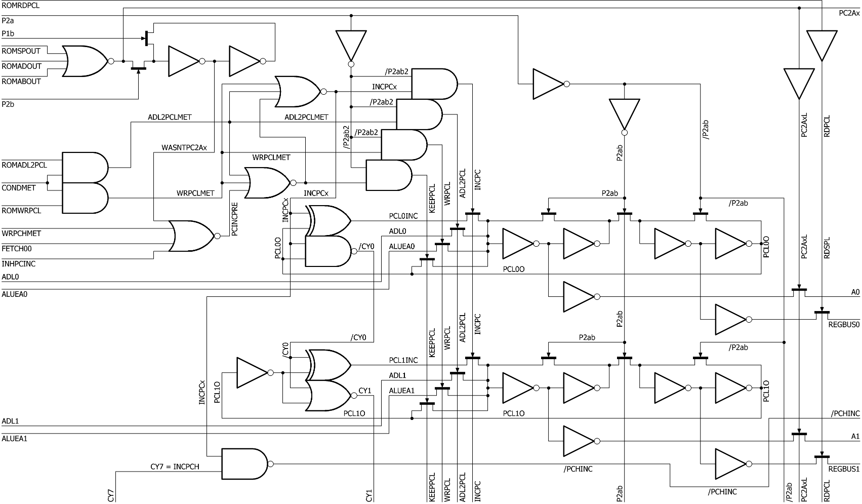
Register PC is a master slave flip-flop and has its own incrementer. PCL register can be written to from ALUEA* bus (when ROMWRPCL and CONDMET are high) or from ADL (when ROMADL2PCL and CONDMET are high) or incremented. It is written to or incremented at the end of P1.
PC register is incremented automatically at the end of each P1 cycle if this is not supressed by INHPCINC signal or PC is not being written to or fake BRK for NMI or IRQ is not being fetched or AB or AD or SP is not being put on address bus.
It can be output to register bus (REGBUS*) by active ROMRDPCL signal and to address bus (A*) when none of AB, AD or SP is put there (enabled by PC2AxL signal). While output to register bus comes from slave flip-flop, the output to the address bus comes from master stage so that it can be put there ahead - in the middle of PHI1 phase.
/PCHINC signal is shown here, it is derived from INCPCx and carry from last bit of incrementer (CY7).
Register PCH
ROM signals: ROMRDPCH, ROMWRPCH, ADJPCH
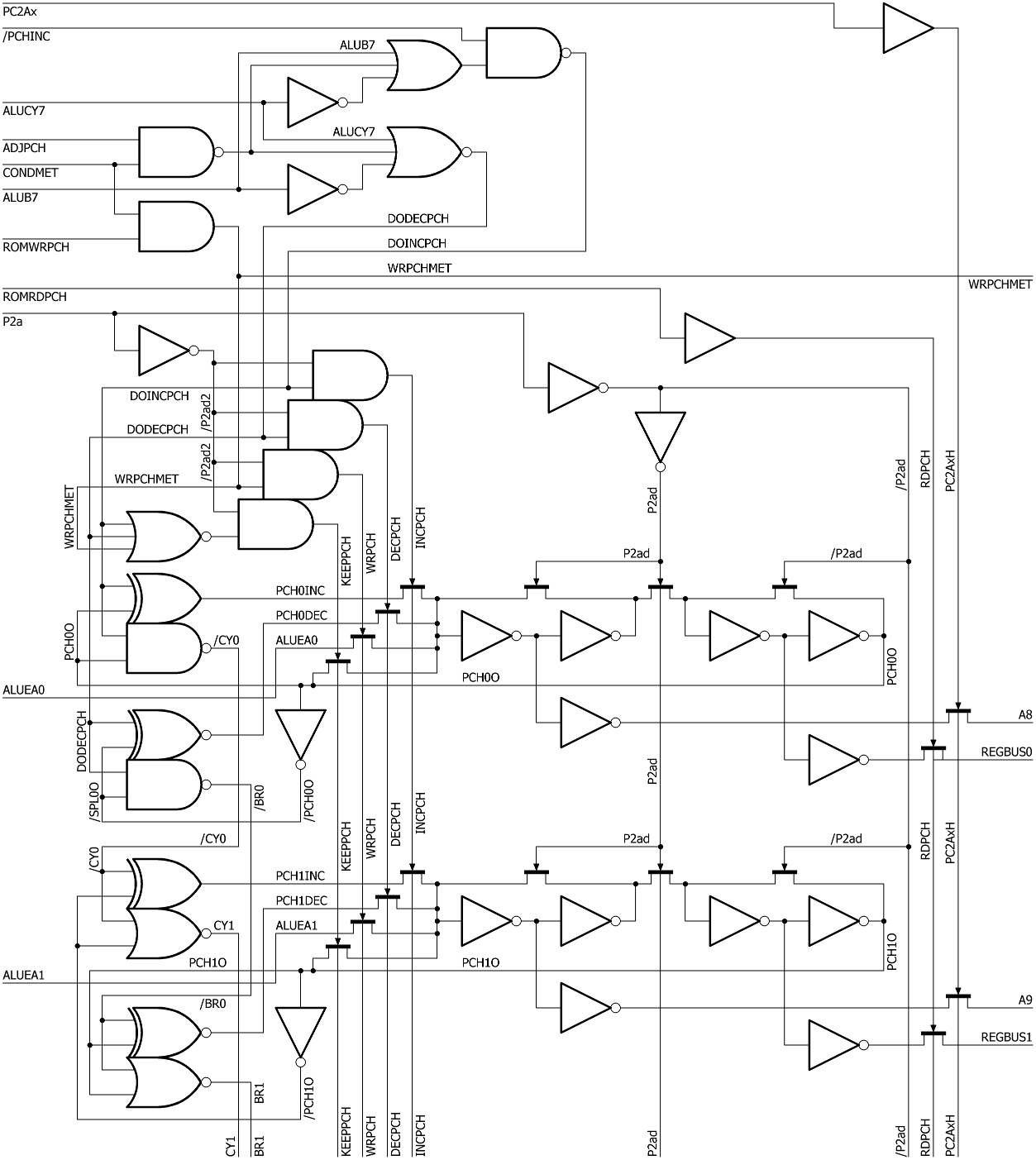
Besides the incrementer, register PCH has its own decrementer. It is used in relative jumps with 8 bit displacement. This logic is activated by ADJPCH signal (providing CONDMET is high). When ALUB7 is low, (i.e. jump forward) and ALUCY7 is high the PCH is incremented. Analogically when ALUB7 is high (i.e. jump back) and ALUCY7 is low, PCH is decremented.
Analogically to PCL, also PCH can be written to from ALUEA* bus (when ROMWRPCH and CONDMET are high).
For automatic incrementing the same logic as for PCL works and PCH is incremented when /PCHINC signal is low. This signal was explained in previsou picture.
And in the same way as PCL, also PCH can be output to register bus (REGBUS*) by active ROMRDPCH signal and to address bus (A*) when none of AB, AD or SP is put there (enabled by PC2AxH signal derived from PC2Ax coming from previous picture). And just like for PCL - while output to register bus comes from slave flip-flop, the output to the address bus comes from master stage so that it can be put there ahead - in the middle of PHI1 phase.
Register SPL
ROM signals: ROMSPOUT, ROMDECSP, ROMINCSP, ROMRDSPL, ROMWRSPL
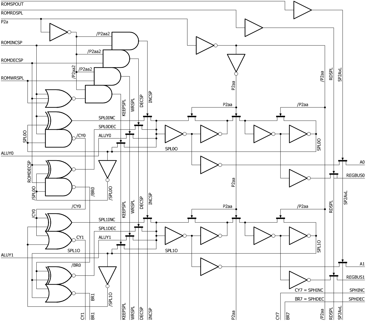
Register SP is a master slave flip-flop and has its own incrementer and decrementer. SPL register can be written to from ALUY* bus when ROMWRSPL is high. Similarly it can be incremented when ROMINCSP is high and decremented when ROMDECSP is high. It is written to or incremented at the end of P1.
As only lowest two bits of the registers are shown, similarly to register PCL the carry bit from the last stage of the incrementer (CY7) is routed as signal SPHINC to register SPH. And similarly the borrow bit from the last stage of the decrementer (BR7) is routed as signal SPHDEC to regester SPH.
SPL register can be output to register bus (REGBUS*) by active ROMRDSPL signal and to address bus (A*) using signal ROMSPOUT. While output to register bus comes from slave flip-flop, the output to the address bus comes from master stage so that it can be put there ahead - in the middle of PHI1 phase.
Register SPH
ROM signals: ROMWRSPH, ROMRDSPH
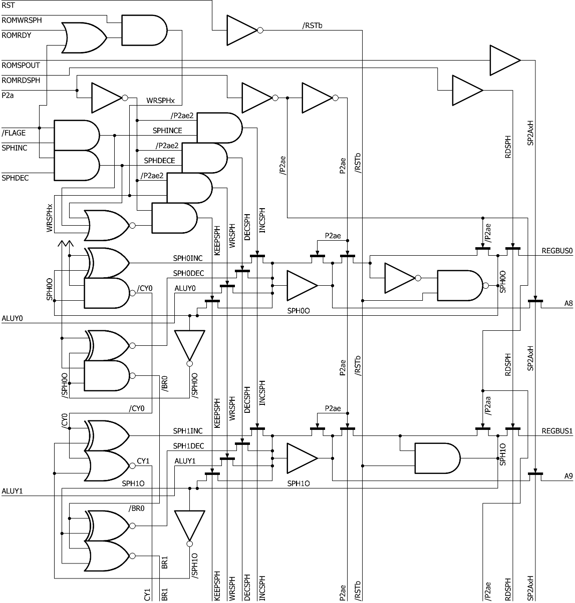
SPH register can be written to from ALUY* bus when ROMWRSPH is high. It can be incremented when SPHINC nad /FLAGE signals are high and decremented when SPHDEC and /FLAGE are high. This means that when flag E is set the upper half of SP register remains unchanged. It is written to or incremented at the end of P1.
After reset when signal RST is high is this register forced to value $01 for maintaining compatibility with 6502.
WRSPH signal is derived from ROMWRSPH. ROMWRSPH signal is used in RTN and TYS instructions. In TYS case WRSPH is activated even if flag E is set. This is not the case for RTN instruction, when flag E is set SPH remains unchanged.
SPH register can be output to register bus (REGBUS*) by active ROMRDSPH signal and to address bus (A*) using signal ROMSPOUT. While output to register bus comes from slave flip-flop, the output to the address bus comes from master stage so that it can be put there ahead - in the middle of PHI1 phase.
A* pads (address bus), A* signals
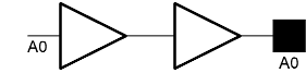
External address bus amplifies and copies everything what is on internal address bus.
Obviously there are 8 copies of this schematic, one for each A* pad.
PROG pad (unconnected)
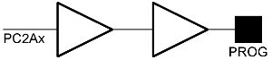
This pad indicates that PC is being output on the address bus. It could help with memory management but it is not connected. Physically it is between pad A7 and pad A8.